07/31/2019
Compound semiconductor technology applicable to high-capacity optical telecommunication and terahertz wirelessNTT Device Technology Laboratories
Overview
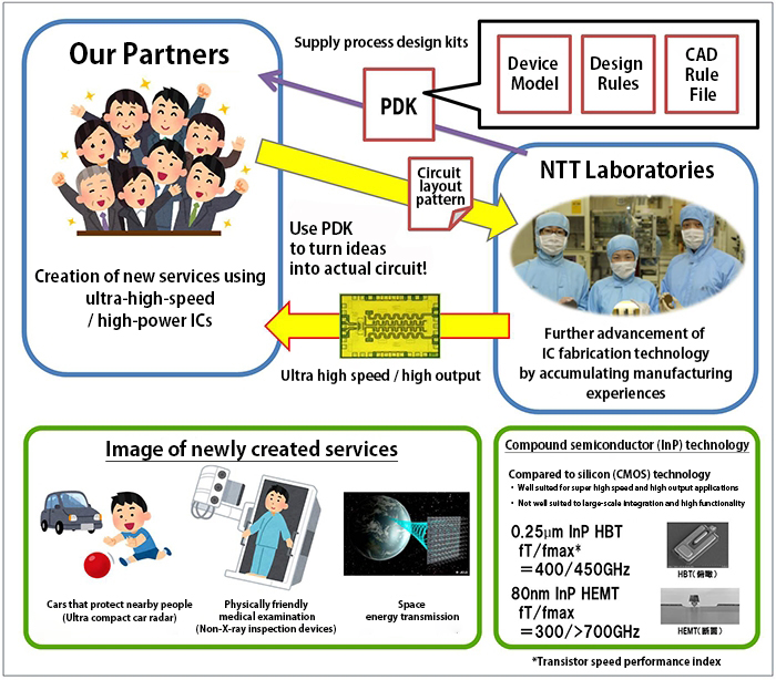
NTT Laboratories starts a collaboration project to make their developed ultra-high-speed IC fabrication technology, which is based on the most advanced InP compound semiconductor R&D process, open. NTT calls for collaborating partners and distribute process design kits (PDK) to all partners. NTT aims to support partners in realizing their designed ICs with cutting edge compound semiconductor process technology, and in creating new services and new industries that use ultra-high-speed ICs. NTT also expect successive advancement of the InP technology though the collaboration.
Background & Existing Issues
Silicon-based ICs generally features highly functionality through large-scale integration exemplified CMOS, but there is a limit to boosting the operating speed and output power. InP-based ICs are not as well suited to high integration, but because they can achieve higher speeds and higher output than silicon, they are expected to serve as complementary technologies.
Advantages of this technology
- World class ultra-high speed InP compound semiconductor integrated process
- Can realize IC with a bandwidth being twice that of silicon technology (InP HBT)
- Can realize IC that opens up the terahertz band (InP HEMT)
- Enables prototyping of ultra-high-speed analog IC that is impossible with silicon technology
- PDK required for IC design is available
- High reliability in anticipation of future commercial use
Use Scenes
- Prototyping and development of ultra-high speed analog ICs
- Verification of new services and applications with newly designed ultra-high speed ICs
- Verification of new services / applications using existing ultra-high speed ICs
Diagram
Glossary
CMOS
Complementary metal oxide semiconductor. CMOS are used when realizing large-scale ICs, such as CPU, GPU and DSP featuring multiple function and complicated processing. This type of circuit is often used for high-capacity optical transmission and reception because of its available massive signal processing. Although scaling down in CMOS accelerates its operating speed, compound semiconductors are superior in terms of high speed and high output.
InP
Indium phosphide. This is a group III-V compound semiconductor consisting of indium and phosphorus. It is used to realize functions for applications that require to generate and handle high speed and high output power signal.
HBT
Heterojunction bipolar transistor
HEMT
High Electron Mobility Transistor
Department in charge
NTT Device Technology Laboratories - Photonics-Electronics Convergence Laboratory