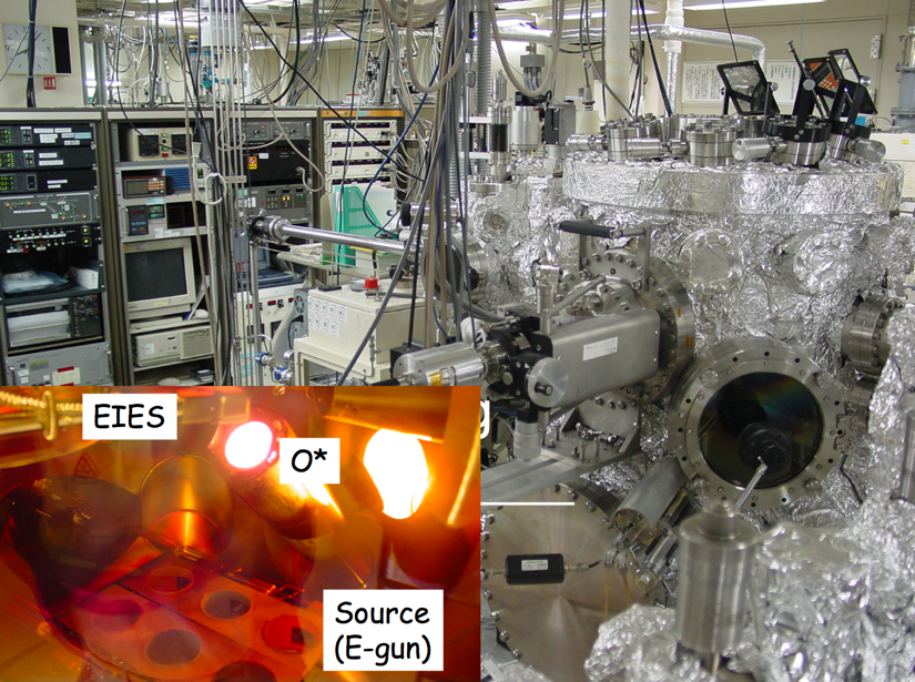
Novel oxide/nitride grown by molecular beam epitaxy
The fascinating properties one is confronted with in condensed matter physics, e.g. high-Tc superconductivity, are best dealt with a tool, i.e. oxide MBE, that allows for manipulations of materials at the atomic level. Our customized oxide MBE system yields high-quality thin films of complex transition metal oxides, their artificial superlattices, and brand-new materials resulting in novel states of matter, and are even applicable to the material research of complex nitrides.
[1] A. Ikeda et al., Phys. Rev. Mater. 3, 064803 (2019)
[2] Y. Krockenberger et al., ACS Omega 6, 21884-21891 (2021)
[3] A. Ikeda et al., ACS Appl. Electron. Mater., 4, 2672-2681 (2022)
[4] K. Takiguchi et al., Phys. Rev. B, 112, 224520 (2025)
[5] K. Takiguchi et al., arXiv:2607.28909 (2026)
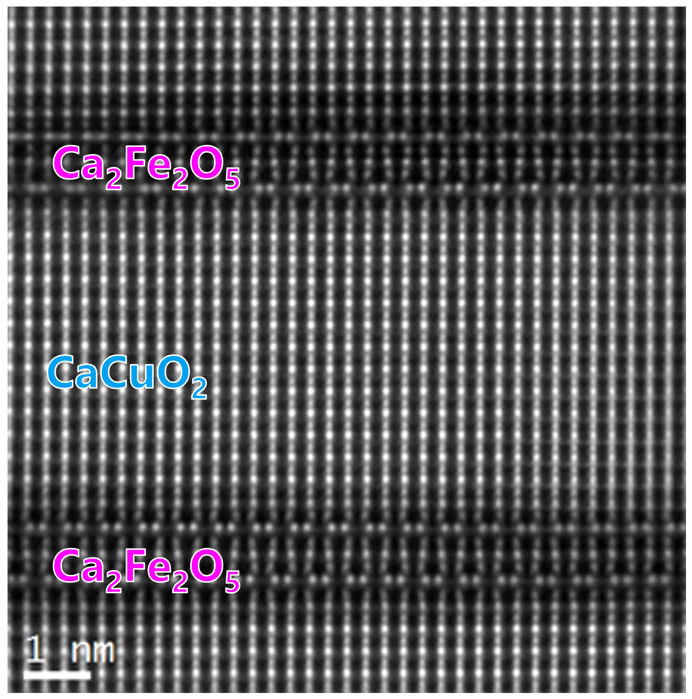
Creating Artificial Heterostructures to Harness Topological Electronic States
We study unusual electronic states arising from the topology of materials, with the aim of developing materials for next-generation spintronics and quantum information technologies. Using our advanced thin-film growth techniques, we combine magnetic materials, semiconductors, and superconductors with atomic-scale precision, then investigate the electronic states that emerge at their interfaces. This work explores new routes toward energy-efficient spintronic devices while advancing fundamental research into Majorana quasiparticles.
[1] Y. Tanaka et al., Appl. Phys. Lett. 124, 072408 (2024)
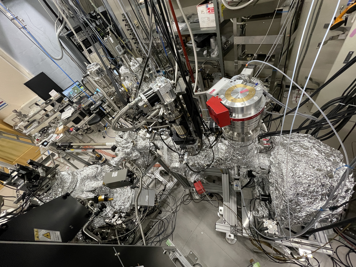
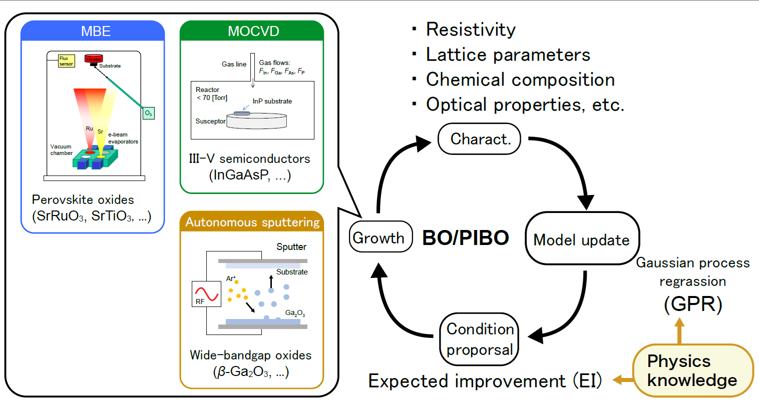
Autonomous Thin-Film Growth through Materials Informatics
We are developing autonomous thin-film growth processes by combining materials informatics with automated experimental technologies. In thin-film materials research, growth parameters such as temperature, pressure, and source supply rates strongly affect crystalline quality, composition, and physical properties, making process optimization highly complex. To overcome this challenge, our group has established closed-loop experimental workflows in which machine learning proposes growth conditions, films are synthesized and characterized, and the resulting data are used to update the model. Our core technologies are Bayesian optimization (BO), which efficiently identifies promising conditions from a limited number of experiments, and Physics-informed Bayesian Optimization (PIBO), which incorporates physical laws and empirical knowledge to accelerate the search. We also develop robust algorithms that account for experimental failures and stagnation in local optima, enabling autonomous optimization in real crystal growth processes. These approaches have been applied to MBE, MOCVD, and autonomous sputtering systems, covering materials such as perovskite oxides, III-V compound semiconductors, and wide-bandgap oxides, and have contributed to improved material functionality and the exploration of new physical properties. Beyond optimization, we analyze data accumulated through autonomous experiments to extract human-interpretable and reusable growth rules and process knowledge. By integrating automation, machine learning, and physical understanding, we aim to accelerate materials and device development and establish a foundation for next-generation autonomous materials research.
[1] Y. K. Wakabayashi et al., APL Mater. 7, 101114 (2019).
[2] K. Takiguchi et al., Nat. Commun. 11, 4969 (2020).
[3] Y. K. Wakabayashi et al., npj Comput. Mater. 8, 180 (2022).
[4] W. Kobayashi et al., npj Comput. Mater. 11, 36 (2025).
[5] Y. K. Wakabayashi et al., arXiv:2602.22531 (2026).