Akira
Fujiwara, Dr. Eng.
Updated on Oct 1, 2020 Japanese
version is here.
HOME PAGE of NTT Basic Res. Labs
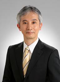 Akira Fujiwara was born in Japan, 1967. He received the B.S., M.S.,
and Ph.D. degrees in applied physics from The University of Tokyo, Japan, in
1989,1991, and 1994, respectively. His Ph.D. thesis
was entitled "Resonant electron capture in semiconductor quantum
wells". In 1994, he joined LSI Laboratories, Nippon Telegraph and
Telephone (NTT) Corporation, Kanagawa, Japan. He moved to the Basic Research Laboratories
(BRL) in 1996. He was a guest researcher at National Institute of Standards and
Technology (NIST), Gaithersburg, USA during 2003-2004. For 2006-2020, He was a
group leader of Nanodevcies
Research Group, NTT BRL. For 2007-2015, He was a Distinguished Technical
Member, NTT BRL. For 2012-2020, he served as an Senior
Manager of
Physical Science Laboratory. Since 2015, He is a NTT Senior
Distinguished Scientist. In 2011-2014 he was supported by the funding
program for Next
Generation World-Leading Researchers (NEXT Program), JSPS. He is now a
leader of the 2018-2022 JSPS
KAKENHI S (Quantum Standards and Ultimate Precision Measurements Based on Single
Electrons) .He is a IEEE fellow and a JSAP (the Japan
Society of Applied Physics) Fellow.
Akira Fujiwara was born in Japan, 1967. He received the B.S., M.S.,
and Ph.D. degrees in applied physics from The University of Tokyo, Japan, in
1989,1991, and 1994, respectively. His Ph.D. thesis
was entitled "Resonant electron capture in semiconductor quantum
wells". In 1994, he joined LSI Laboratories, Nippon Telegraph and
Telephone (NTT) Corporation, Kanagawa, Japan. He moved to the Basic Research Laboratories
(BRL) in 1996. He was a guest researcher at National Institute of Standards and
Technology (NIST), Gaithersburg, USA during 2003-2004. For 2006-2020, He was a
group leader of Nanodevcies
Research Group, NTT BRL. For 2007-2015, He was a Distinguished Technical
Member, NTT BRL. For 2012-2020, he served as an Senior
Manager of
Physical Science Laboratory. Since 2015, He is a NTT Senior
Distinguished Scientist. In 2011-2014 he was supported by the funding
program for Next
Generation World-Leading Researchers (NEXT Program), JSPS. He is now a
leader of the 2018-2022 JSPS
KAKENHI S (Quantum Standards and Ultimate Precision Measurements Based on Single
Electrons) .He is a IEEE fellow and a JSAP (the Japan
Society of Applied Physics) Fellow.
Research Interests
Physics and application of low-dimensional structures
Silicon nanostructures
and their application to nanodevices
Single-electron devices
and their applications
Education
1991 M.S. in Applied
Physics, The University of Tokyo
1994 Ph.D. in Applied
Physics, The University of Tokyo
1989 B.S. in Applied
Physics, The University of Tokyo
Employment
2015- Senior Distinguished Scientist, NTT BRL
2012- Senior Manager of Physical Science Laboratory, NTT BRL
2007-2015 Distinguished technical member, NTT BRL
2006- Group leader of Nanodevices Research Group,
NTT BRL
1996 NTT Basic Research Laboratories (BRL)
1994 NTT LSI Laboratories
Professional Activities
2017.10-2023.9 Science Council of Japan, member
2016 & 2012 & 2019 Examiner of Ph.
D. thesis, UNSW
2014 & 2011 &
2008 Examiner of Ph. D. thesis, Tokyo
Tech.
2013.4-2014.3 Visiting Professor, Hokkaido University
2012 Examiner of Ph. D.
thesis, UNSW
2011.4-2012.3 Japanese Society of Applied Physics(JSAP) Executive
Director
2010.4-2011.3 Japanese Society of Applied Physics(JSAP) Director
2003.7-2004.7 Guest
researcher at the National Institute of Standards and Technology (NIST), Gaithersburg,
MD, USA
2007.8 Lecturer(Non-Full-time), The University of Tokyo
Awards and Honors
JSAP fellow, 2020.9.8
JSAP Silicon Technology Division Paper Award, 2020
IEEE fellow, 2018.1.1
Prizes for Science and Technology, the Minister of Education, Culture, Sports, Science and Technology (MEXT), 2017
Japanese Journal of
Applied Physics (JJAP) Paper Awards, 2013
The Young Scientists’
Prize, the Minister of MEXT (Ministry of Education, Culture, Sports, Science, and
Technology), 2006
Japanese Journal of Applied
Physics (JJAP) Paper Awards, 2006
Japanese Journal of Applied
Physics (JJAP) Paper Awards, 2003
SSDM (International
Conference on Solid State Devices and Materials) Paper Award, 1999
SSDM (International Conference
on Solid State Devices and Materials) Young Researcher Award, 1998
Committee/International Conference Activities
Co-chair of
International Symposium on Nanoscale Transport and Technology ISNTT 2015,
Atsugi, Nov. 2015.
Co-chair of Silicon Quantum
Electronics Workshop, Takamatsu, Aug. 3-4, 2015.
Program vice chair of
Int. Conf. on Solid State Devices and Materials (SSDM2014), Tsukuba, Sept.
2014.
Co-chair of
International Symposium on Nanoscale Transport and Technology ISNTT 2013,
Atsugi, Nov. 2013.
Program vice chair of
Int. Conf. on Solid State Devices and Materials (SSDM2013), Fukuoka, Sept.
2013.
Program vice chair of
APPC12(the 12th Asia Pacific Physics Conference), Makuhari, Japan, July, 2013.2007.8
Co-chair of Workshop
on Innovative Devices and Systems (WINDS) , Hawaii, USA, Dec. 2-7 2012.
Special committee of Emerging Research Devices
WG, STRJ (Semiconductor Technology Roadmap Committee of Japan) 2008.10-
Government Fund
2018-2022 JSPS KAKENHI S (Quantum Standards and Ultimate Precision
Measurements Based on Single Electrons)
2011-2014 The Funding Program
for Next Generation World-Leading Researchers (NEXT Program), JSPS
CV (as of 2020.10.1)
Curriculum
Vitae (CV) incl. publication lists etc.
Publication data
(as of 2018.6.15)
http://www.researcherid.com/rid/A-6648-2012
Total: 171 papers, Average Citations 19 h-index 32
First author: 17 paper, Average Citations 32.94 h-index 11
Google
Scholor Citations (automatically updated)
Recent selected
papers/international conferences (updated on Oct 1, 2020)
Single-electron transfer and dynamics, Tunable-barrier single-electron transistor and
double quantum dots, Single-dopant
device
[1]
S. P. Giblin, E. Mykkänen, A. Kemppinen, P. Immonen, A. J. Manninen, M. Jenei, M. Möttönen, G. Yamahata, A.
Fujiwara and M. Kataoka, Realisation of a quantum current standard at liquid helium
temperature with sub-ppm reproducibility, Metrologia
doi.org/10.1088/1681-7575/ab72e0 (2020).
[2]
(Published in Nature Nanotech. !)G. Yamahata, S. Ryu, N. Johnson,
H-S. Sim, A. Fujiwara, and M. Kataoka, Picosecond
coherent electron motion in a silicon single-electron source, Nature
Nanotechnology 14, 1019–1023 (2019).
[3]
N. Johnson, G. Yamahata, and A. Fujiwara,
Measurement of the curvature and height of the potential barrier for a dynamic
quantum dot, Appl. Phys. Lett. 115, 162103 (2019).
[4]
S. Giblin, A. Fujiwara, G. Yamahata, M. H.
Bae, N. Kim, A. Rossi, M. Möttönen, and M. Kataoka, Evidence for universality of tunable-barrier
electron pumps, Metrologia 56, 044004 (2019).
[5]
G. Yamahata, S. P. Giblin, M. Kataoka, and T. Karasawa, and A.
Fujiwara, High-accuracy current generation in the nanoampere regime from a
silicon single-trap electron pump, Scientific Reports 7, 45137 (2017).
[6]
G. Yamahata, S. P. Giblin, M. Kataoka, T. Karasawa, and A.
Fujiwara, Gigahertz single-electron pumping in silicon with an
accuracy better than 9.2 parts in 107, Appl. Phys. Lett. 109,
013101 (2016).
( See
http://www.npl.co.uk/news/record-speed-and-accuracy-achieved-with-single-electron-pumps
)
[7]
G. Yamahata, T. Karasawa,
and A. Fujiwara, Gigahertz single-hole transfer in Si
tunable-barrier pumps, Appl. Phys. Lett. 106, 023112 (2015).
[8]
G. Yamahata, K. Nishiguchi, and A.
Fujiwara, Gigahertz single-trap electron pumps in silicon, Nat. Commun. 5, 5038 (2014).
[9]
G. Yamahata, K. Nishiguchi, and A. Fujiwara: Accuracy
evaluation and mechanism crossover of single-electron transfer in Si
tunable-barrier turnstiles Phys. Rev. B 89, 165302 (2014).
[10]
G. Lansbergen, Y. Ono and A. Fujiwara: Donor based single electron
pumps with tunable donor binding energy, Nano Lett. 12 763−768
(2012).
[11] G. Yamahata, K. Nishiguchi, and A. Fujiwara: Accuracy
evaluation of single-electron huttle transfer in Si
nanowire metal-oxide-semiconductor field-effect transistors, Appl. Phys. Lett. 98,
222104 (2011).
[12] S. Miyamoto, K.
Nishiguchi, Y. Ono, K. M. Itoh, and A. Fujiwara: Resonant escape over an
oscillating barrier in a single-electron ratchet transfer, Phys. Rev. B 82,
033303 (2010).
[13] S. Miyamoto, K. Nishiguchi,
Y. Ono, K M. Itoh, and A. Fujiwara: Escape dynamics of a few electrons in a
single-electron ratchet using silicon nanowire metal-oxide-semiconductor
field-effect transistor, Appl. Phys. Lett. 93, 222103 (2008).
[14] A. Fujiwara, K.
Nishiguchi, and Y. Ono: Nanoampere charge pump by single-electron
ratchet using silicon nanowire metal-oxide-semiconductor field-effect
transistor: Appl. Phys. Lett. 92, 042102 (2008).
[15] H. W. Liu, T.
Fujisawa, Y. Ono, H. Inokawa, A. Fujiwara, K.
Takashina, and Y. Hirayama: Pauli-spin-blockade transport through a silicon
double quantum dot, Phy. Rev. B 77, 073310 (2008).
[16]
M. A. H. Khalafalla, Y.
Ono, K. Nishiguchi, and A. Fujiwara: Identification of single and coupled
acceptors in silicon nano-field-effect transistors, Applied Physics Letters 91,
263513 (2007).
[17] A. Fujiwara, H. Inokawa,
K. Yamazaki, H. Namatsu, Y. Takahashi, N. M.
Zimmerman, and S. B. Martin: Single electron tunneling transistor with tunable
barriers using silicon nanowire metal-oxide-semiconductor field-effect
transistor, Appl. Phys. Lett. 88 053121 (2006).
[18]
A.
Fujiwara, N. M. Zimmerman, Y. Ono, and Y. Takahashi: Current quantization due
to single-electron transfer in Si-wire charge-coupled devices, Appl. Phys. Lett. 84, 1323-1325 (2004).
[19]
A.
Fujiwara and Y. Takahashi: Manipulation of elementary charge in a silicon
charge-coupled device, Nature 410, 560-562 (2001).
Single-electron detection and counting
statistics / stochastic resonance
[1]
(Published in Nature Com. !) K Chida, S. Desai, K Nishiguchi, and A Fujiwara: Power generator
driven by Maxwell's demon, Nat. Commun. 8, 15310
(2017).
[2]
K Chida, K Nishiguchi, G Yamahata, H Tanaka, A Fujiwara: Thermal-noise suppression
in nano-scale Si field-effect transistors by feedback
control based on single-electron detection, Appl. Phys. Lett. 107, 073110, 2015 (2015).
[3]
P. A. Carles, K Nishiguchi, and A
Fujiwara: Deviation from the law of energy equipartition in a small
dynamic-random-access memory, Jpn. J. Appl. Phys. 54,
06FG03 (2015).
[4]
K. Nishiguchi, Y. Ono, and A. Fujiwara: Single-electron thermal
noise, Nanotechnology 25, 275201 (2014).
[5] K. Nishiguchi, H.
Yamaguchi, A. Fujiwara, H. S. J. van der Zant, and G.
A. Steele, Wide-bandwidth charge sensitivity with a radio-frequency
field-effect Transistor, Appl. Phys. Lett. 103, 143102 (2013).
[6] K. Nishiguchi and
A. Fujiwara: Detecting signals buried in noise via nanowire transistors
using stochastic resonance, Appl. Phys. Lett. 101, 193108 (2012).
[7] K. Nishiguchi and
A. Fujiwara: Single-Electron Stochastic Resonance Using Si Nanowire Transistors,
Jpn. J. Appl. Phys. 50, 06GF04 (2011)..
[8]
K. Nishiguchi, N. Clement, T. Yamaguchi, and A.
Fujiwara: Si nanowire ion-sensitive field-effect transistors with a shared
floating gate, APPLIED PHYSICS LETTERS 94,
163106 (2009).
[9]
K. Nishiguchi and A. Fujiwara: Single-electron
counting statistics and its circuit application in nanoscale field-effect
transistors at room temperature, Nanotechnology
20 175201 (2009).
Functional nanotransistors,
sensors, molecular electronics
[1]
(Published in Nature Com !) H. Firdaus, T.
Watanabe, M. Hori, D. Moraru, Y. Takahashi, A.
Fujiwara, and Y. Ono, Electron aspirator using electron–electron scattering
in nanoscale silicon, Nature Communications 9, 4813 (2018)
[2]
(Published in Nature Materials !) R. Sivakumarasamy,
R. Hartkamp, B. Siboulet,
J.-F. Dufreche, K. Nishiguchi, A. Fujiwara,
and N. Clément, Selective-layer-free Blood Serum Ionogram based on Ion-specific
Interactions with a Nanotransistor, Nature Materials
17 464 (2018).
[3]
N. Clement and A. Fujiwara, Molecular diodes: Breaking the Landauer limit, Nat. Nanotech. 12, 725 (2017).
[4] N. Clément,
K. Nishiguchi, J. F. Dufreche, D. Guerin, A. Fujiwara, and D. Vuillaume, Water Electrolysis and Energy Harvesting with
Zero-Dimensional Ion-Sensitive Field-Effect Transistors, Nano Lett. 13,
3903−3908 (2013).
[5] I. Mahboob, K.
Nishiguchi, A. Fujiwara, and H. Yamaguchi, Phonon Lasing in an
Electromechanical Resonator , Phys. Rev. Lett. 110
127202 (2013).]
[6] N. Clément, K.
Nishiguchi, J. F. Dufreche, D. Guerin, A. Fujiwara,
and D. Vuillaume, A silicon nanowire ion-sensitive
field-effect transistor with elementary charge sensitivity, Appl. Phys. Lett. 98, 014104 (2011).
[7] I. Mahboob, E. Flurin, K. Nishiguchi, A. Fujiwara, and H.
Yamaguchi: Nature Communications 2, 198 doi:10.1038/ncomms1201
(2011).
[8]
N. Clément, K. Nishiguchi, A. Fujiwara and D. Vuillaume: One-by-one trap activation in silicon nanowire
transistors, Nature Communications 1 DOI:10.1038/ncomms1092
(2010).
Silicon quantum well and optical properties
[1]
J. Noborisaka, K. Nishiguchi, A. Fujiwara:
Electric tuning of direct-indirect optical transitions in silicon, Scientific
Reports 4, 6950 (2014).
[2]
J. Noborisaka, K.
Nishiguchi, Y. Ono, H. Kageshima, and A Fujiwara: Strong
Stark effect in electroluminescence from phosphorous-doped silicon-on-insulator
metal-oxide-semiconductor field-effect transistors, Appl. Phys. Lett. 98, 033503 (2011).
[3]
J. Noborisaka, K.
Nishiguchi, H. Kageshima, Y. Ono, and A Fujiwara:
Tunneling spectroscopy of electron subbands in thin
silicon-on-insulator metal-oxide-semiconductor field-effect transistors, Appl.
Phys. Lett. 96, 112102 (2010).
Physics of Si 2DEG and valley physics in collaboration with Prof. Hirayama
(Tohoku Univ. ) and Dr. Takashina (Univ. of Bath) , Dr. Vincent Renard (CEA)
[1]
V. T. Renard, B. A. Piot, X. Waintal, G. Fleury, D. Cooper, Y. Niida,
D. Tregurtha, A. Fujiwara, Y. Hirayama and K.
Takashina, Valley polarization assisted spin polarization in two dimensions,
Nat. Commun. 6, 7230 (2015).
[2] V. T. Renard, I. Duchemin, Y. Niida, A. Fujiwara, Y. Hirayama and K. Takashina, Metallic behaviour in SOI quantum wells with strong intervalley scattering, Scientific reports | 3 : 2011 |
DOI: 10.1038/srep02011 (2013).
[3] K. Takashina, Y. Niida, V. T. Renard, B. A. Piot,
D. S. D. Tregurtha, A. Fujiwara, and Y. Hirayama,
Phys. Rev. B 88, 201301(R) (2013).
[4] Y. Niida, K. Takashina, Y. Ono, A. Fujiwara and Y. Hiryama: Electron and
hole mobilities at a Si/SiO2 interface with
giant valley splitting, Appl. Phys. Lett. 102, 191603 (2013).
[5] K. Takashina, Y. Niida, V. T. Renard, A. Fujiwara,
T. Fujisawa, K. Muraki, and Y.Hirayama:
Impact of Valley Polarization on the Resistivity in Two Dimensions, Phys. Rev.
Lett. 106, 196403 (2011).
[6] K. Takashina, K. Nishiguchi,
Y. Ono, A. Fujiwara, T. Fujisawa, Y. Hirayama, and K. Muraki:
Electrons and holes in a 40 nm thick silicon slab at cryogenic temperatures, APPLIED PHYSICS LETTERS 94, 142104
(2009).
[7] Y. Niida,
K. Takashina, A. Fujiwara, T. Fujis awa, and Y.
Hirayama: Spin splitting of upper electron subbands
in a SiO2/Si(100)/SiO2 quantum well with in-plane magnetic field, APPLIED PHYSICS LETTERS 94,
142101 (2009).
Invited talk:
[1]
A.
Fujiwara, G. Yamahata, N. Johnson, S. Ryu, H-S. Sim, and M. Kataoka,
Fast electron dynamics in a silicon dynamic quantum dot, Int. Workshop on Cool Electrons
in Flatlands (CEF2020) (June 15-24, 2020, Catania, Italy, held as virtual
workshop)
[2]
A.
Fujiwara, Silicon nanodevices for metrology and sensor applications, IEEE
Nanotechnology Materials and Devices Conference (IEEE NMDC2019) (Oct.. 27-30,
2019, Stockholm, Sweden)
[3]
A.
Fujiwara, Ultimate electronics with silicon nanowire MOSFETs, Workshop on
Innovative Nanoscale Devices and Systems (WINDS) (Nov. 25-30, 2018, Hawaii,
USA)
[4]
A.
Fujiwara, G. Yamahata, K. Chida,
and K. Nishiguchi, Tunable-barrier electron pump for quantum current standards
and information-to-energy converters China-Japan International Workshop on
Quantum Technologies, QTech2018 (Aug 23-24, 2018, Hefei, China).
[5]
A.
Fujiwara, Ultimate electronics with control of single electrons, 7th Summer School
on Semiconductor/Superconducting Quantum Coherence Effect and Quantum
Information (August 27-29, 2017, Shuzenji, Japan).
[6]
A.
Fujiwara, K. Nishiguchi, G. Yamahata, and K. Chida, Ultimate electronics with control of single
electrons, EM-NANO2017 (June 18-21, 2017, Fukui, Japan).
[7]
A.
Fujiwara, K. Nishiguchi, G. Yamahata, and K. Chida, Ultimate Single Electronics with Silicon Nanowire
MOSFETs, 2017 Silicon Nanoelectronics Workshop (June
4-5, 2017, Kyoto, Japan).
[8]
A.
Fujiwara, G. Yamahata, K. Nishiguchi, S. P. Giblin,
and M. Kataoka, Gigahertz single-electron pump for
quantum current standard, 33rd ICPS
(Beijing, 31 July- 5 August, 2016)
[9]
A. Fujiwara, G. Yamahata, and K. Nishiguchi, Gigahertz Single-Electron Pump
towards a Representation of the New Ampere, 2015 SSDM (Sapporo, 27-30
September, 2015).
[10] A. Fujiwara, G. Yamahata, J. Noborisaka, and K. Nishiguchi, Nanoscale Silicon MOSFET for
Metrology and Valleytronics Applications, 2015
UK-Japan Silicon Nanoelectronics and Nanotechnology
Symposium (Southampton, 9-10 July, 2015).
[11]
(Plenary talk) A. Fujiwara,
Silicon single-electron devices for ultimate electronics, EURAMET DC &
Quantum Metrology Meeting (Bern, 27-29 May 2015)
[12] A. Fujiwara, K. Nishiguchi, G. Yamahata, Silicon nanowire MOSFETs for diverse
applications, The 6th IEEE International Nanoelectronics
Conference 2014 (INEC2014) (Sapporo, July 28-31, 2014)
[13] (Plenary talk) A. Fujiwara, Silicon-based
nanodevices for diverse applications, 39th Int. Conf. on Micro and
Nano Engineering (MNE) (London, UK, Sept. 16-19 2013).
[14] A. Fujiwara, G. Yamahata,
K. Nishiguchi, G. P. Lansbergen and Y. Ono: Silicon
Single-Electron Transfer Devices: Ultimate Control of Electric Charge, 2012
Silicon Nanoelectronics Workshop (June 2012, Hawaii,
USA).
[15] A. Fujiwara, K. Nishiguchi, and Y. Ono:
Single electron transfer technology using Si nanowire MOSFETs, 2010 International Symposium on Atom-scale
Silicon Hybrid Nanotechnologies for ‘More-than-Moore E&
‘Beyond CMOSEEra (March 1 E 2, 2010,
Southampton, UK), Program and Abstracts, pp. 19 E20.)
[16] A. Fujiwara, K. Nishiguchi and Y. Ono:
Single-electron devices based on silicon nanowire MOSFETs, Trends in
Nanotechnology (TNT2009) p.39 (September 7-11, 2009,Barcelona)
[17] A. Fujiwara, K. Nishiguchi and Y. Ono:
Silicon Nanowire MOSFETs and Their Application to Single-Electron Devices,
International Conference on Nanoscience and Technology (ChinaNANO)
2009, p. 50-51 (September 1-3, 2009,Beijing)
[18] A. Fujiwara, K. Nishiguchi, Y. Ono, H. Inokawa, and Y. Takahashi: Silicon Single-Electron Devices
and Their Applications, 2008 Tera-level NanoDevices (TND) Technical Forum (Soul, 2008.10.17).
[19] A. Fujiwara and Y. Takahashi: Si nano-devices using an electron-hole system, 2nd International Conference on
Semiconductor Quantum Dots (QD2002) (2002.9).
[20] A. Fujiwara and Y. Takahashi: Si nano-devices using an electron-hole system, Proceedings of 5th Europian
Workshop on Low Temperature Electronics, (Journal de Physiqye
IV, 12, No.Pr3), Ed. F Balestra, (WOLTE-5) pp. Pr3-85-Pr3-92 (2002.6).
[21] A. Fujiwara, K. Yamazaki, and Y. Takahashi:
Silicon Single-electron CCD, 2001 Int. Micreprocess and Nanotechnology Conference (MNC) pp.
278-279 (2001.10).
[22] A. Fujiwara, Y. Takahashi, K. Yamazaki, H. Namatsu, M. Nagase, K. Kurihara,
and K. Murase
Single-electron devices: recent attempts towards high performance and
functionality, 1999 Int. Conf. Solid
State Devices and Materials (SSDM) pp. 248-249 (1999).
[23] A. Fujiwara, Y. Takahashi, K. Yamazaki, H. Namatsu, M. Nagase, K. Kurihara,
and K. Murase: Silicon single-electron devices
fabricated by pattern-dependent oxidation (PADOX), Sweden-Japan Joint QNANO Workshop (1998).
[24] A. Fujiwara, Y. Takahashi, K. Yamazaki, H. Namatsu, M. Nagase, K. Kurihara,
and K. Murase: Silicon single-electron devices
fabricated by pattern-dependent oxidation (PADOX), International Symposium on Formation, Physics and Device Application of
Quantum Dot Structures (QDS98), (1998).
Selected first-author papers
[1] A. Fujiwara, K. Nishiguchi, and Y. Ono:
Nanoampere charge pump by single-electron
ratchet using silicon nanowire metal-oxide-semiconductor field-effect
transistor: Applied Physics Letters 92, 042102 (2008).
[2]
A. Fujiwara, H. Inokawa,
K. Yamazaki, H. Namatsu, Y. Takahashi, N. M.
Zimmerman, and S. B. Martin: Single electron tunneling transistor with tunable
barriers using silicon nanowire metal-oxide-semiconductor field-effect
transistor, Applied Physics Letters 88 053121 (2006).
[3]
A. Fujiwara, N. M. Zimmerman, Y. Ono, and
Y. Takahashi: Current quantization due to single-electron transfer in Si-wire
charge-coupled devices, Applied Physics Letters 84, 1323-1325 (2004).
[4] A. Fujiwara, S. Horiguchi,
M. Nagase, and Y. Takahashi: Threshold voltage of Si single-electron
transistor, Japanese Journal of Applied Physics Part 1-Regular Papers Short
Notes & Review Papers 42, 2429-2433 (2003).
[5] A. Fujiwara, K. Yamazaki, and Y. Takahashi:
Detection of single charges and their generation-recombination dynamics in Si
nanowires at room temperature, Applied Physics Letters 80,
4567-4569 (2002).
[6] A. Fujiwara and Y. Takahashi: Mechanism of
single-charge detection using electron-hole system in Si-wire transistors, Japanese
Journal of Applied Physics Part 1-Regular Papers Short Notes & Review
Papers 41, 1209-1213 (2002).
[7] A.
Fujiwara and Y. Takahashi: Manipulation of elementary charge in a silicon
charge-coupled device, Nature 410, 560-562 (2001).
[8] A. Fujiwara, Y. Takahashi, K. Yamazaki, H. Namatsu, M. Nagase, K. Kurihara,
and K. Murase: Double-island single-electron devices
- A useful unit device for single-electron logic LSI's, IEEE Transactions on
Electron Devices 46, 954-959 (1999).
[9] A. Fujiwara, Y. Takahashi, H. Namatsu, K. Kurihara, and K. Murase: Suppression of effects of parasitic
metal-oxide-semiconductor field-effect transistors on Si single-electron
transistors, Japanese Journal of Applied Physics Part 1-Regular Papers Short
Notes & Review Papers 37, 3257-3263 (1998).
[10] A.
Fujiwara, Y. Takahashi, and K. Murase: Observation of
single electron-hole recombination and photon-pumped current in an asymmetric
Si single-electron transistor, Physical Review Letters 78, 1532-1535 (1997).
[11] A. Fujiwara, Y. Takahashi, K. Murase, and M. Tabe:
Time-Resolved Measurement of Single-Electron Tunneling in a Si Single-Electron
Transistor with Satellite Si Islands, Applied Physics Letters 67,
2957-2959 (1995).
3-1 Morinosato Wakamiya, Atsugi-shi,
Kanagawa, 243-0198 JAPAN